Microsoft-backed startup Lace raises $40M to build atomic-level chipmaking tech
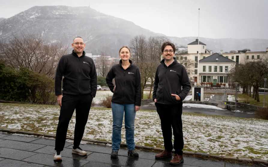
A small team in Norway is taking aim at one of the hardest problems in computing: how to keep shrinking chips as today’s methods approach their limits. Lace Lithography, a Bergen-based startup backed by Microsoft, has raised $40 million to advance a new chipmaking technology that could reshape how advanced processors are built.
Reuters confirmed the funding, reporting, “Lace, a Norway-headquartered chipmaking equipment startup which is backed by Microsoft, has raised $40 million in funding to further develop a technology that could enable significant advances in semiconductor design and manufacturing.”
Modern chips rely on lithography, a process that uses light to etch intricate patterns onto silicon. The entire system has been refined for decades, with companies like ASML supplying the machines that make it possible. Those tools have become the backbone of AI hardware, helping manufacturers pack more transistors into tighter spaces.
Lace is trying a different path. Instead of light, the company uses a beam of helium atoms to draw patterns at a far smaller scale. CEO Bodil Holst says this approach could unlock designs that current systems simply can’t reach.
“Our technology is a way that can potentially expand the roadmap and be an enabler for doing things that would not have been possible otherwise,” Holst said.
Before founding Lace, Holst built her career as a physicist focused on nanoscale imaging and molecular-beam lithography. She holds an affiliated professorship at the University of Bergen, where her research has spanned 2D materials, smart surfaces, and advanced characterization techniques.
The numbers help explain the ambition. The helium beam Lace is working with has a width of around 0.1 nanometers. By comparison, the extreme ultraviolet light used in today’s most advanced lithography systems operates at roughly 13.5 nanometers. For context, a human hair is about 100,000 nanometers wide.
That gap matters. Smaller features mean more transistors on a chip, which translates into higher performance for AI workloads. If Lace can deliver on its promise, chipmakers could move closer to what Holst describes as “ultimately atomic resolution.”
Researchers in the field are paying attention. John Petersen, Scientific Director of Lithography at Imec, said the approach could allow manufacturers to build features an order of magnitude smaller than what is possible today, pushing into territory that has long felt out of reach.
The timing is not accidental. Governments and investors are pouring money into semiconductor innovation as demand for AI hardware continues to climb. A new wave of startups is trying to carve out space in a market long dominated by a handful of players, with ASML holding a commanding position in lithography systems.
Lace’s $40 million Series A round was led by Atomico, with participation from Microsoft’s venture arm M12, Linse Capital, the Spanish Society for Technological Transformation, and Nysnø. The company has already built early prototypes and plans to move toward a pilot system inside a test fabrication plant by 2029.
That timeline leaves plenty of work ahead. Turning a lab breakthrough into a production-ready tool is one of the toughest transitions in the chip industry. Still, if helium atom lithography proves viable at scale, it could extend the life of Moore’s Law in a way many thought was slipping out of reach.
For now, Lace is positioning itself as a quiet contender in a field that rarely changes overnight. The stakes are high, and so is the potential upside.
Trending Now

Top Tech News Today, May 5, 2026